◀ MOTIVATION ▶
It was the summer of '24, and I had just finished up my first year of Electrical and Computer Engineering at Purdue University. I had a lot of time left rolling around, as unlike most of my friends, I wasn't able to score a summer internship. So, I did what I always do best: I made my own. I went to LinkedIn, created a business page, and hired myself as a Min Works Hardware Design summer intern. After announcing my fortunate opportunity, I immediately got to work.This wasn't going be just another hobby project. It would be a demonstration of all the knowledge and skills I've acquired over the years as a hobbyist and engineering student. I wanted to incorporate all the different domains of ECE I was interested in, such as power supply design, digital systems, and signal processing. It didn't take long to come up with something: I set out to design an automotive data acquisition system for high-speed processing and transmission of data through CAN.
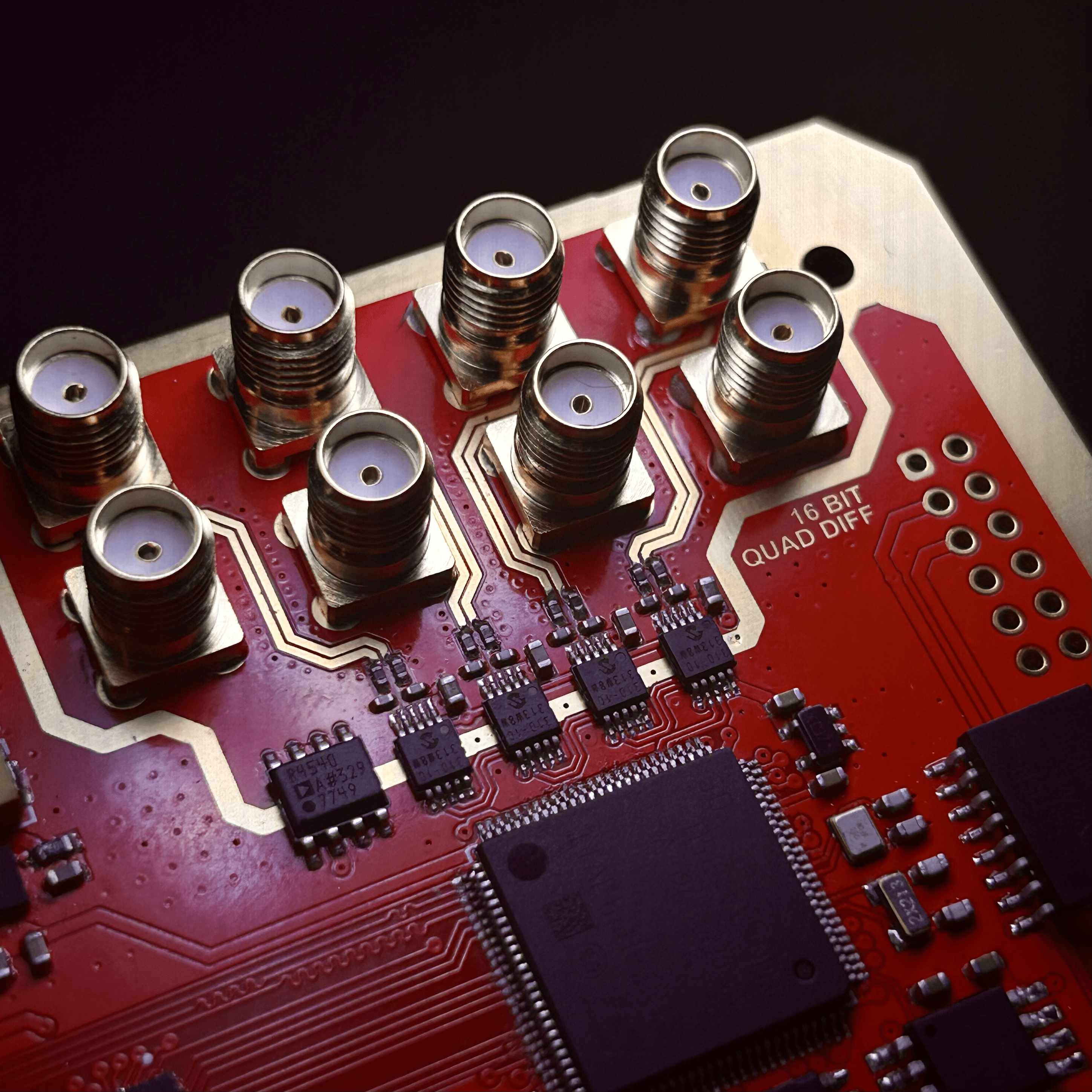
Introducing B.O.S.S., short for
Basically, an
Overengineered
Super
Sampler.
A system for the acquisition, processing, and transmission of high-fidelity signals.
◀ SPEC LIST ▶
Before I start, I would be fully transparent and clarify that THIS DESIGN IS NOT FULLY WORKING!!! The ICE40UP5K FPGA is not working as of right now (8/27/2024), but I've checked the schematic and checked voltages countless times with no faults yet to be found, so I'm still confident I will be able to get it running someday. My school schedule's quickly picking up and soon I'll have no time for any hobby work, which is why I'm writing this write-up now.
◀ DESIGN ▶
I started jotting down ideas around three weeks before my spring semester ended. Even before I wrote anything down, three things were for sure:1. It was going to incorporate an FPGA.
2. It was going to have a proper power supply.
3. It was going to be an exercise in mixed-signal PCB design, and I was going to make it as precise and as accurate as possible.
New goals and objectives developed constantly during the process of board design and layout. Later, I started implementing my own custom communication interface between the FPGA and STM32, as well as designing a more robust PSU than planned to meet certain automotive ISO standards.
Unlike Time Machine Mk. 8, the design was a pretty straightforward process once I had all major component choices and placements locked in. While I often found myself re-routing a section or moving parts around, the design as a whole didn't really change much from my initial concept sketch to the final product.
◀ HARDWARE ▶
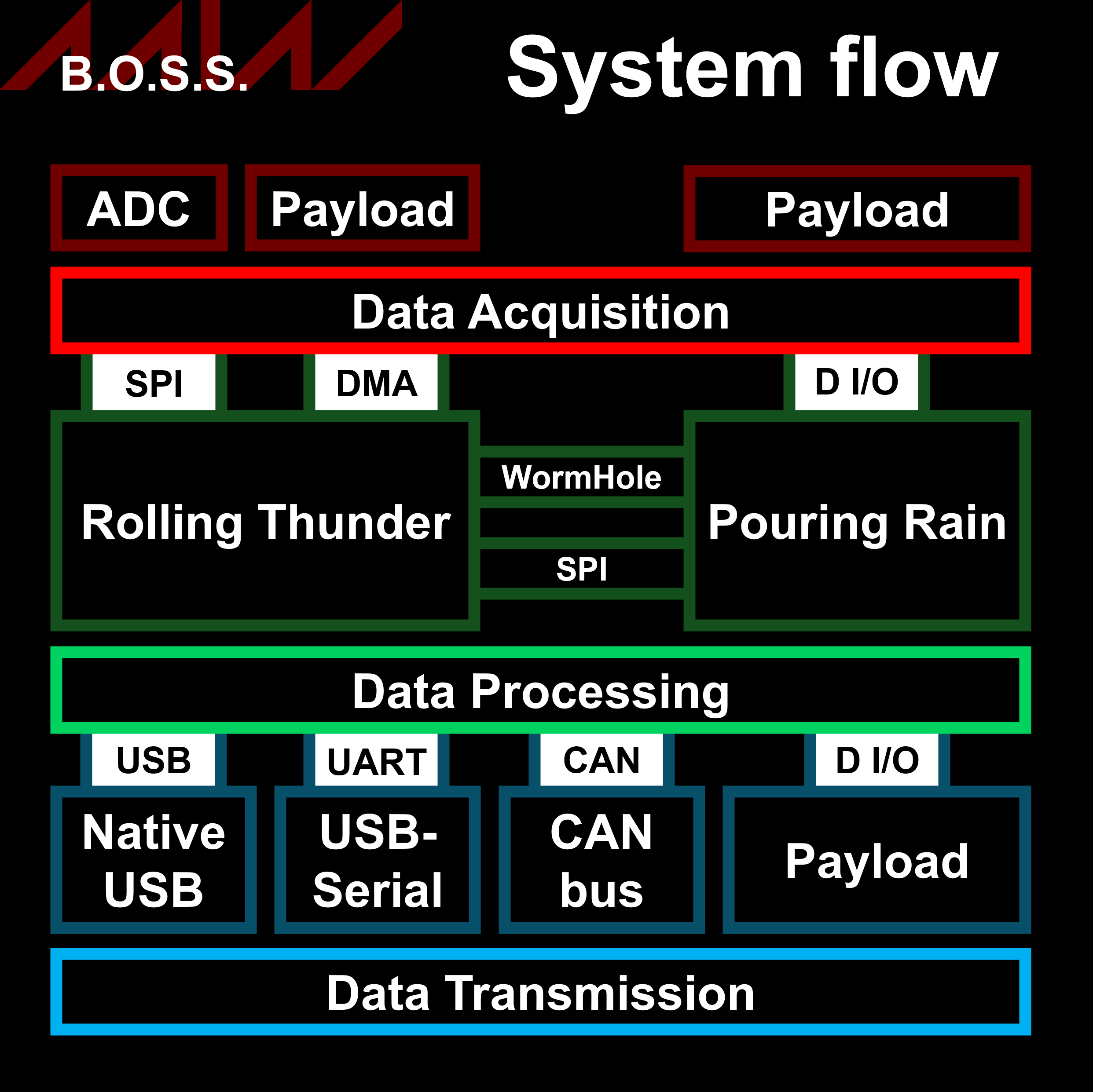
SYSTEM OVERVIEW

STM32H743VGT6 - "ROLLING THUNDER"
ICE40UP5K - "POURING RAIN"
FT2232HL
MCP33131D
POWER SUPPLY - "MJÖLNIR"
LAYER STACKUP
asdf
asdf
asdf
asdf
asdf
